A Streamlined Manufacturing Experience
From design and prototyping to production and assembly, we offer a comprehensive suite of services to ensure the success of your PCBA project.
- PCB and PCBA Manufacturing
- Component Sourcing & Procurement
- Supply Chain Management & Problem-Solving
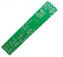
Long PCB
The manufacturing and assembly process of long PCBs is similar to traditional PCBs, but requires longer substrate materials and special production equipment to match the size requirements. Additionally, in order to ensure the stability and reliability of the circuit board that the process control is required. SCSPCBA can make PCBs up to 1.5 meters long.

Peelable Mask PCB
Peelable Mask PCB is a special type of printed circuit board that utilizes peelable mask material during the manufacturing process. The peelable mask is a temporary protective layer covering the PCB, usually a polymer material. It is applied in areas that need to be protected, such as pads, golden fingers and specific components, etc.
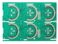
Carbon Ink PCB
Carbon Ink PCB is a special type of printed circuit board which printed with carbon ink. Compared to traditional copper foil circuits, carbon Ink PCBs have poor conductivity, low power transfer capability and limitations on high-frequency signals, etc. However, carbon ink PCBs have a wide range of applications in the field of flexible electronics, particularly in applications that prioritize cost-effectiveness, flexibility and environmental protection.
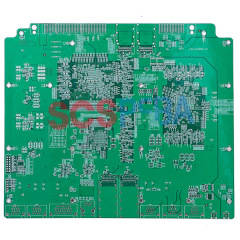
Impedance Controlled PCB
SCSPCBA focuses on quality control and process control to ensure that the produced impedance controlled PCBs have stable performance and consistent impedance values. You can rely on SCSPCBA's professional capability and experience to obtain high-performance impedance PCB. Whether it's in communication, computer, medical equipment or other high frequency and high speed applications, SCSPCBA can provide reliable solutions for impedance controlled PCBs.
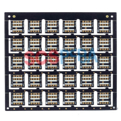
Controlled Depth Drilling PCB
Controlled depth drilling PCB (back drilling PCB) is a type of printed circuit board with special holes. It uses specific drilling techniques in the manufacturing process to ensure that the depth of the drilled holes meets the predetermined requirements. This type of hole design can be used for install specific components, pins, or other connection parts that require depth control.
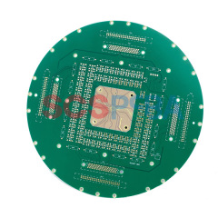
Countersink Hole PCB
Countersunk hole PCBs are typically used in applications that require mounting screws or bolts, and require a flat surface. This design allows the head of the screw or bolt to be embedded inside the hole so that it is flush with the PCB surface, thereby avoiding the interference of the protruding screw head on other components or external structures.
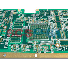
Edge Plating PCB
The manufacturing process of edge copper plated PCB involves exposing the edge portion of the PCB and coating it with thin copper.
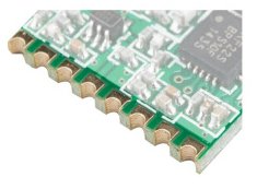
Plated Half Holes PCB
The manufacturing process of plated half holes PCB is similar to that of regular PCBs, but there is a difference in the drilling process. When producing plated half holes PCBs, the vias will only partially through the thickness of the PCB rather than going through the entire board. Then, the half hole wall is coated with a conductive material, typically copper. This provides the plated half holes with a conductive inner surface, which can be used for the installation of pins, sockets, or other types of connectors. By inserting these components into the plated half holes and performing soldering or other connection methods, a reliable electrical connection can be established between the PCB and other devices.
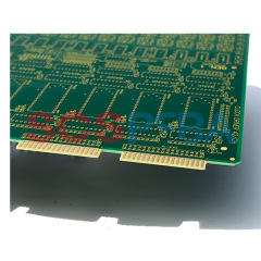
Gold Fingers PCB
Gold fingers are typically located on the edge of the PCB, and they are designed and arranged in specific shapes and patterns to facilitate connection with other devices or plug-ins.
Heavy Copper PCB
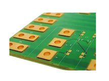
Heavy copper PCB is made on traditional FR4 substrate by increasing the copper thickness to achieve high current and power transfer and to provide better heat dissipation.
Rigid and Flexible PCB
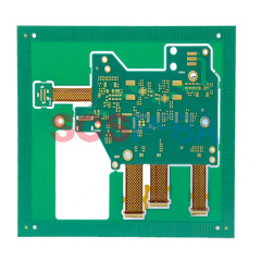
Rigid-Flex PCB is combined with rigid PCB and flexible PCB. The flexible portion can be bent, folded or flexed while the rigid portion provides stable support and connections.
HDI PCB/Blind and Buried Vias PCB
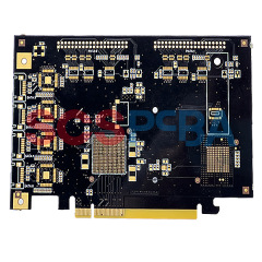
The HDI process is a high-density interconnection technology used to manufacture high-performance and high-density printed circuit boards (PCBs). HDI technology achieves more compact and complex circuit layouts by increasing the number of layers, reducing the line widths and spacing, and adopting advanced manufacturing processes.
VIA IN PAD PCB
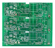
Via in Pad is a technology commonly used in PCB design, which allows the pins of electronic components to be directly connected to the vias located in pad. It provides a more compact and reliable connection method.
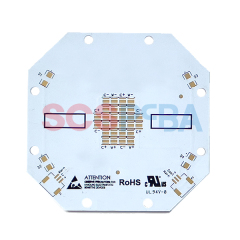
Metal Base PCB
A Metal Base PCB (Printed Circuit Board) is a type of circuit board that has a metal base layer, usually made of aluminum or copper, instead of the traditional epoxy or fiberglass substrate found in standard PCBs. The metal base provides several advantages, making it suitable for specific applications where enhanced thermal performance is crucial.